THZ RESPONSE
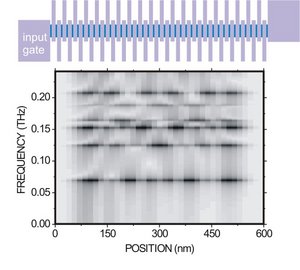
Simulated THz response spectrum of a multi-gate GaAs nanowire FET (channel diameter=20nm, length=600nm, gate oxide=10nm, 4 electrons).
So far, common characterization methods for FETs involve signal frequencies from DC up to 100 GHz. However, typical energy scales of quantized states in realistic nanowire FETs are on the order of a few meV corresponding to the THz frequency range. We therefore propse signals in the THz regime to directly probe quantum transitions between few-electron states within a nanowire FET. For the first time, we have simulated the intra-band THz response of such devices by means of a novel many-body quantum approach (BBCI) [1,2], taking quantization and few-electron Coulomb interaction effects beyond mean-field into account. Combining this spectroscopic approach with a multi-gate design [2], we obtain spatially resolved information about the electronic spectra inside the FET, far beyond the limitations of standard characterization methods.
The figure shows a schematic sketch of the considered nanowire FET with multiple gate segments and the THz spectrum of a realistic example. Such a spatially resolved spectrum can be interpreted as a fingerprint of the concrete electronic structure, which might prove useful in future experimental realizations as a means to characterize nanoscale devices for information technology.
Further reading:
[1] cond-mat/0609540 (2006)
[2] Phys. Rev. B 77, 125436 (2008)
(We are not affiliated in any way with companies/persons mentioned above. All brand names and trademarks are property of their respective owners. Wir distanzieren uns ausdrücklich von jeglichen Inhalten fremder Webseiten, auf die durch unser Webangebot verwiesen wird, und schließen eine Haftung für Inhalte fremder Webseiten aus.)