Student Micro Foundry (SMF)
| Project name: | HSRM Student Micro Foundry (SMF) – A student-run teaching and learning platform for microelectronics |
| Department: | Engineering – Applied Physics (interdisciplinary with ING-ITE and DCSM) |
| Project lead: | B.Eng. Manuel Robert Handta Prof. Dr. Markus Bender |
| Project participants: | ING-AP: Prof. Dr. Stefan Kontermann, Prof. Dr. Daniel Münstermann, M.Sc. Martin Sommer, Dipl.-Ing. Alexander Dörr, B.Sc. Dennis Hunter, B.Sc. Florian Neff, B.Sc. Simon Kreuels ING-ITE: Matthias Harter DCSM: Prof. Dr. Steffen Reith, Prof. Dr. Marc Stöttinger, M.Sc. Tim Henkes |
| Location: | RheinMain University of Applied Sciences, Am Brückweg 26, 65428 Rüsselsheim am Main, Building A – Room U05 |
| Duration: | 01.04.2026 – 31.03.2028 |
| Funding body or client: | RheinMain University of Applied Sciences – Funds for improving the quality of study conditions and teaching (QSL) |
Project description
The HSRM Student Micro Foundry (SMF) creates a student-run teaching and learning platform in which students design, fabricate and characterise simple microelectronic devices themselves. The goal is a continuous process chain from ASIC/HDL design through lithography, doping and metallisation to the electrical characterisation of real devices.
The SMF closes a key gap in teaching: microelectronics is often taught theoretically or through simulation, while physical fabrication usually remains invisible due to high equipment costs. Through didactically controlled and reproducible processes, students learn how functional structures emerge from material, layout, process control and metrology – from pn junctions and diodes to transistors and, in the long term, simple integrated circuits.
In addition to using existing infrastructure, a central goal is to build our own open process equipment, such as lithography units, spin coaters, doping and annealing processes, probe station extensions and characterisation setups. Inspired by international Open/HackerFab approaches, these systems are documented openly, built reproducibly and continuously improved. Students thus learn not only how to fabricate microelectronics, but also to understand the laboratory infrastructure required for it.
Roadmap
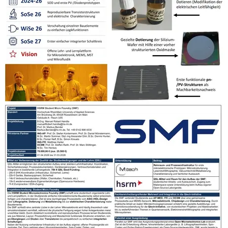
- 2024–26: Feasibility study – pn junctions, spin-on dopant (SOD) and first PV/diode prototypes
- Summer 2026: Reproducible transistor structures and electrical characterisation
- Winter 2026/27: Interconnecting individual devices into simple logic functions
- Summer 2027: First simple integrated circuit
- Vision: Open teaching and learning platform for microelectronics, MEMS, microsystems technology and microfluidics
Interdisciplinary added value
The SMF connects students from AP-MED, ITE and DCSM through a shared process chain covering MEMS sensors, microelectronics, chip design and characterisation. Hands-on work with real microtechnology processes provides targeted training and doctoral preparation for the Qtech initiative – from student projects and master's theses to advanced topics in quantum sensing, electron beam lithography and integrated microsystems.
Funding
The QSL funds enable the structured development of a stable teaching infrastructure: coordination, safety concept, process documentation (SOPs), additional equipment, consumables and integration into existing courses. This creates a sustainable platform for project-based teaching, theses and future projects in MEMS, microfluidics, sensor technology and sensor-integrated microsystems.